NVIDIA's GeForce GTX 690


We all by now know that the GTX690 is comprised of 2 GTX680s all on a single slot PCB that should if by all rumors come true seriously dominate the GPU world. That is the basic quick mock-up of the new card, but that only scratches the surface of what really lies under the hood of this new product. Many of the technologies used in how this card is made are coming to light with this launch as well so this should be some interesting reading for you folks who love to read about tech. Well sit back a spell and let's dig a bit deeper into NVIDIA’s latest entry into the VGA foray and see just what all the fuss is about with this new Dual GPU monster called the GTX690.


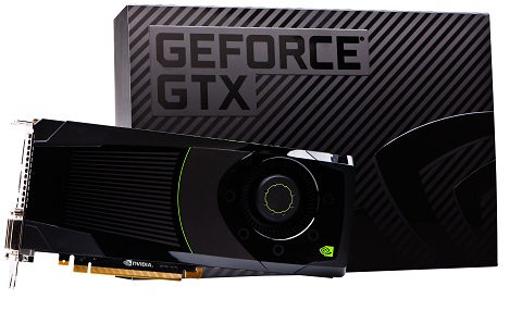
Here we have it! The GeForce GTX 690, The pinnacle or flagship and crown jewel of the Kepler crown!  This board is the Fastest and most efficient GPU ever built and being a card that is basically two GTX680’s on a single card we really cannot doubt that claim.  We have tested the GTX 680 already and the performance, acoustics, thermals and power draw are all large step forward for NVIDIA.


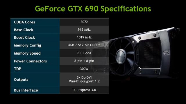
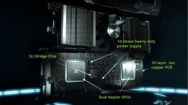
Here we see the specs directly from NVIDIA and we would be lying to say it's not impressive as normally when we see a dual GPU card its not the flagship single GPU doubled up and is usually cut down or lower end model GPU to allow for a lower thermal output which can fit the thermal solution fitted to the card, not to mention the power the PCB can realistically deliver. With how efficient the GTX 680 is and greater thermal performance we have seen this is likely why NVIDIA was able to stuff two of these GPUs in this package.


The GTX 690 offers a full 3072 CUDA cores when combining the two GPUs add to that each GPU carries 2GB of framebuffer for a total of 4GB.  Keep in mind that since this card is 2 cards basically in SLI mode which means that the framebuffer has the same information on both sets so the units will utilize 2GB total framebuffer and therefore depending on the loading of the card in some heavy texture loads we could see this 2GB get used up in the right situation (such as Skyrim with some hi res texture packs and mods). The base clock on the GPUs have been turned down a bit from the default GTX 680 1006 to a more conservative 915 MHz so just under a 100 MHz drop and the boost clock drops from 1058 to 1019 which means NVIDIA definitely got more aggressive with the boost clock to ensure that when available this card should be right at a SLI pair of GTX 680’s performance level.  Memory on the GTX 690 is still at 6Gbps which means it should be right on par with 680 as well.  One thing we notice is that the GTX690 is rated at 300W whereas dual 680’s are rated at 195W a piece which total out to 90W less than using a GTX680 pair but we find rather nice for such a powerful offering. 


A breakdown of the cooling system and what makes it run. Once removed we can see that under the cover we have dual vapor chamber coolers (1 per GPU) which help sap heat away from the GPU and exhaust it to the passing airflow. The center mounted fan is similar to the style we have seen on the GTX590 and is mounted to a base plate which also works as a heat spreader for the VRM, memory and other critical components. The base plate has special grooves or “channels” as NVIDIA references them which helps the cooling airflow dissipate the heat away from the cooling plate.  One thing to note is that since the fan is a center mounted axial design were going to see some heat put into the case by the inward GPU as the airflow is exhausted from the end of the card, this in most systems will make a menial difference but in some cases or under extreme stress for a long time the heat exhausted could build up so the need for chassis airflow definitely exists.


After passing the cooling components we get to a render of the board components.  Needless to say this is where things get interesting and definitely what we've been waiting for.  These are the parts that make the magic happen and keep games churning along.  This card has dual full spec Kepler GPUs doing the grunt work being fed by a 10 phase hi performance VRM.  Bridging the dual GPUs is handled by a PLX Bridge chip which we will look at in more detail soon.  All of this is mounted to a super stout 10 layer PCB sporting 2oz copper content to make sure there should be no signaling or performance issues no matter the load or stress placed on it.


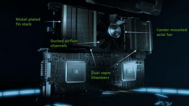
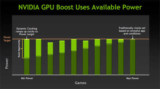
GPU boost is one of the new technologies we have already seen on the GTX680.  This is NVIDIA’s way of modulating clock speeds to allow for higher “boost clocks” when TDP and thermals is still within limits and there is headroom to allow for even more performance from the card.  The GTX 680 had a mild boost clock maximum of 52MHz which has enough for a nice little boost in gameplay but the GTX 690 really surprised us as it offers  a boost clock of 104MHz over the base clock putting it within grabbing distance of the GTX680 boost clocks. The Kepler GPU is designed around a new generation of stream multiprocessing which in essence is a NVIDIA's way of refining the way it makes the cards work by removing the previously seen “processor clock” which was double the speed of the GPU clock and instead taking the GPU and completely revamping it to add more CUDA cores at the lower speed to allow a much better performance per watt ratio than could have been done with the previous implementation.


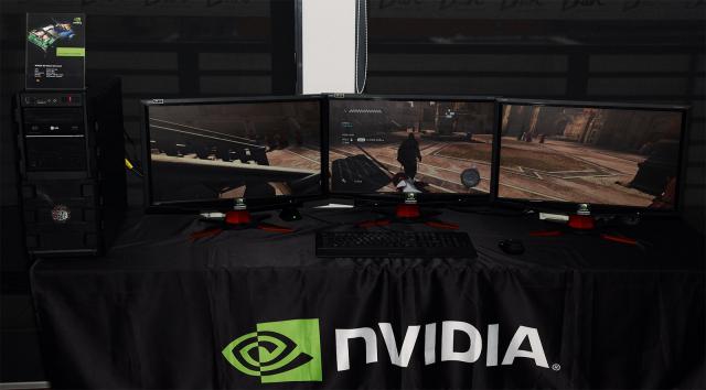
The ability to run 3 3D monitors in a very high resolution on a single card was first seen on the GTX680, but now with twice the power you can run at high resolutions with all the bells and whistles enabled and still get solid gameplay without hiccups or stutters. With 4GB of available memory Multi-Monitor support has never been better for NVIDIA fans and the GTX690 can run 4 monitors off a single card, 3 by way of DVI ports and 1 via the Mini Display Port. This also gives the user a wide variety of monitors to use such as the 30’’ Dell that works very well using the Display Port connection.


If I could just summarize this entire GTX 690 launch with one word that word would be simply WOW! Everything about the new NVIDIA GTX 690 just speaks volumes of how much research and development went into this card design, as it will change things on the playing field. From the outstanding looks of the stellar performance one can only surmise that NVIDIA has been for once actually holding back the bit so to speak as this card is what change is all about.

GIGABYTE : Digital Power Engine (3D Power)


GIGABYTE Z77 series motherboards take advantage of an exclusive All Digital PWM controller array, to deliver power to the board's 3rd generation Intel® Core™ processor. Using entirely digital controllers means that more precise power delivery to the motherboard's most power hungry and energy sensitive components is possible. These components include the CPU, VTT, processor graphics and memory, without doubt the most important components on your motherboard. This All Digital Power system, with Precise Auto Voltage Compensation, provides you with exceptional control over the component power delivery on your GIGABYTE 7 series motherboard. 


GIGABYTE 3D Power: Digital Voltage, Frequency and Phase Control 
Utilizing an exclusive All Digital controller array, GIGABYTE's 3D Power features precise Auto Voltage Compensation to deliver a steady flow of power to the system, no matter the loading. With digital controllers for the CPU (Vcore), VTT, processor graphics and memory (DDR), users can make real-time adjustments with the exclusive GIGABYTE 3D Power Utility, that include settings such as OVP (Over Voltage Protection), Load-line Calibration and on-the-fly PWM frequency adjustment.

GIGABYTE 3D Power Utility

Users can enjoy a fully interactive 3D utility that facilitates adjustment of the 3 dimensions that control the power delivery to your CPU and Memory: Voltage, Phase and Frequency. These parameters are crucial to how the digital PWM supplies power to critical areas of the motherboard and can help users quickly obtain the highest, most stable overclock.


3D Power: Voltage Control
Voltage parameters can be modified within 3D Power, including load line calibration of the CPU. By adjusting load line calibration, Vdroop can be avoided, maintaining optimal voltages levels despite increasing current levels. OVP (over voltage protection) can also be adjusted to change default protection range of the CPU, IGP, VTT and system memory.


3D Power: Phase Control
Users can calibrate OCP (Over Current Protection) for the CPU, integrated memory controller and system memory power levels. This allows the Phase control to deliver even more power to the system when needed.


3D Power: Frequency Control
GIGABYTE's all digital PWM allows for adjustable frequency control via the International Rectifier PWM controller. 3D Power frequency control allows users to change the PWM controller frequency so that the CPU VRM can adjust power delivery speeds more quickly. Users can also adjust the PWM spectrum or maximum and minimum overall frequencies.


Ivy Bridge Unveiled : A look Inside the Intel Core i7 3770K


Ivy Bridge has been a Buzz word that has been tossed around the world, and one that has everyone in anticipation of just what the hell Intel has up their sleeves for the desktop environment, and finally the long awaited day has arrived where we can actually legally show off just what all the hype and hoopla was all about. Many sites have already violated NDA, which is a legal statement by Intel addressing the time and date of releasing their information to the public, but we held fast waiting for the actual stated deadline to arrive before breaking the news to you good folks. It sucks to be a legitimate player sometimes as that means towing the line even under pressure.


When it comes to CPUs and their accompanying chipsets there is no company known to man that reaches the levels that Intel does. Always on the forefront of technology and development it is a rare day to see anyone offering them anything but the slightest competition as AMD really does not create a hard competitor for big blue. Everybody is always looking for a better, faster and more affordable solution to solve their computing needs and from entry level to High-End Intel has a solution to fit your need. The big Buzz word for this event is Ivy Bridge and it once again see’s Intel breaking ground and paving the way for a new desktop platform.  Sandy Bridge was a very big market hit and the i7 2500K one of the most sought after CPUs for the overclocker and gamer crowd who have pushed that CPU to its limits squeezing every ounce of performance they could extract from it. 

Intel releases a new set of CPUs to work on their latest Z77 and other Chipset motherboards that offers many new features including a separate chip for the onboard graphics all housed in the same Silicon in a similar fashion to the AMD APU line of products, but one that actually has a pair of balls to back up the video capabilities where the APU uses a low end processors in its mix. That might be good for very entry-level projects, but Ivy is ready for desktop primetime and has both good CPU power and GPU power to boost about. This release will show Intel on a new road that takes your graphics needs very seriously and if they really put their efforts in an all out quest to achieve this the graphics cards companies will have to find new ways to fill in that niche. I am no scientist so I don’t grasp and truly understand all the technology involved in creating a new CPU so I wont even try to convey that, but I do know what works and if it is something I would want to actually own and use.  I am a layman, gamer and enthusiast just like 98% of the people reading this review. With that in mind lets take a closer look at what Intel’s been trying to keep under wraps for months, the new Core i7 3770K.


The Desktop 3rd Generation Intel CoreTM processor family is the next generation of 64-bit, multi-core processors built on 22-nanometer process technology. The processors are designed for a two-chip platform. The two-chip platform consists of a processor and a Platform Controller Hub (PCH) and enables higher performance, lower cost, easier validation, and improved x-y footprint. The processor includes Integrated Display Engine, Processor Graphics, PCI Express ports, and an Integrated Memory Controller. The processor is designed for desktop platforms. The processor offers either 6 or 16 graphic execution units. The number of EU engines supported may vary between processor SKUs. The processor is offered in an 1155-land LGA package, but will not function on previous generation chipset motherboards.

Intel has now shrunk the die size of the of the CPU from 32nm to 22nm just like we have seen the VGA companies doing on the new 6 series from NVIDIA and 7 series from AMD so its no surprise to see the CPUs going in the same direction. Today Intel introduces 10 new CPUS to the desktop market, these are as follows: The Intel CoreTM i7-3770K, i7-3770, i7-3770S, i7-3770T, i5-3570K, i5-3550, i5-3550S, i5-3570T, i5-3450, and i5-3450S processors. We are looking at the i7 3770K the new flagship CPU for the Ivy Bridge platform featuring an unlocked core and HD4000 graphics. The i7 3770K is clocked at 3.5GHz with Turbo Boost to 3.9GHz, has 4 Cores that when used with Hyper-Threading enabled works like 8 cores, and having an unlocked core means that overclockers will have the utmost in flexibility when trying to get the most performance from their CPU. Lower power requirements should also translate into a cooler running CPU as well and with Intel now being 100% behind the entire overclocking movement this new generation of processors should be the most receptive to this process.

Ivy Bridge Special Features

 8-Way MultiTask Processing: Runs 8 independent processing threads in one physical package.            
Intel Turbo Boost Technology 2.01: Dynamically increases the processor frequency up to 3.9 GHz when applications demand more performance. Speed when you need it, energy efficiency when you don’t.            
Intel Hyper Threading Technology: Allows each core of the processor to work on two tasks at the same time providing amazing processing capability for better multitasking, and for threaded applications.            
Intel Smart Cache: 8MB of shared cached allows faster access to your data by enabling dynamic and efficient allocation of the cache to match the needs of each core significantly reducing latency to frequently used data and improving performance.            
CPU Overclocking Enabled (with Intel Z77 Express & Z75 Express Chipsets)
Fully unlocked core multiplier, power, and DDR3 memory ratios enable high flexibility for overclocking.
Graphics Overclocking Enabled (with all Intel 7 Series Chipsets) 5: Unlocked graphics multiplier allows for overclocking to boost the graphics clock speed.            
Integrated Memory Controller: Supports 2 channels of DDR3 1600 memory with 2 DIMMs per channel. Support for memory based on the Intel Extreme Memory Profile (Intel XMP) specification.
Chipset/Motherboard Compatibility: Compatible with all Intel 7 Series Chipsets and selected Intel 6 Series Chipsets6.         
Intel Secure Key: a HW assist processor technology designed to produce high-quality, high-security, high-volume random numbers through an on-chip entropy source that can be used for various security computing demands.            
Intel OS Guard: A HW assist processor technology designed to prevent certain system malware attacks aiming to gain kernel level access to the operating system (OS enabling required).
Intel AES New Instructions (AES-NI) Provides 6 processor instructions that help to improve performance for AES encryption and decryption algorithms.            
Built-in Visuals: New enhanced built-in visual features deliver a seamless visual PC experience for doing everything from simple e-mail to enjoying the latest 3D and HD entertainment.
The built-in visuals suite includes: Intel Quick Sync Video 2.0 Technology: Media processing for incredibly fast conversion of video files for portable media players or online sharing. Intel InTruTM3D9: Stereoscopic 3D Blu-ray playback experience in full HD 1080p resolution over HDMI 1.4 with
3D. Intel Clear Video HD Technology: Visual quality and color fidelity enhancements for spectacular HD playback and immersive web browsing. Intel Advanced Vector Extensions (Intel AVX): Increased performance for demanding visual applications like professional video & image editing. Intel HD Graphics 4000: Brand new graphics architecture delivering full DX11 functionality and up to 2X compute throughput (via increased number of execution units and dual-issue), translating into significant graphics performance enhancements (over 2nd Gen Intel Core processors with HD Graphics 2000/3000) for immersive mainstream gaming on a broader range of titles.

Supported Technologies
 • Intel Virtualization Technology for Directed I/O (Intel® VT-d)
• Intel Virtualization Technology (Intel® VT-x)
• Intel Active Management Technology 8.0 (Intel® AMT 8.0)
• Intel Trusted Execution Technology (Intel® TXT)
• Intel Streaming SIMD Extensions 4.1 (Intel® SSE4.1)
• Intel Streaming SIMD Extensions 4.2 (Intel® SSE4.2) • Intel® Hyper-Threading Technology • Intel® 64 Architecture
• Execute Disable Bit
• Intel Turbo Boost Technology
• Intel Advanced Vector Extensions (Intel® AVX)
• Advanced Encryption Standard New Instructions (AES-NI)
• PCLMULQDQ Instruction
• RDRAND instruction for random number generation
• SMEP – Supervisor Mode Execution Protection
• PAIR – Power Aware Interrupt Routing

Core i7 3770K Computation Performance

In this section of the review we compare the i7 2600K to the i7 3770K in direct CPU computational performance so you can see just what types of performance levels there are between Sandy Bridge and Ivy Bridge. These tests are designed to stress the various aspects of your CPUs total computing power and how they perform under a full load. We ran the i7 2600K at its stock clock speed of 3.4GHz and the 3770K at both its core clock at 3.5GHz and at an overclocked state at 4.6GHz.


 The biggest thing that has happened is something getting smaller as in the new die shrinkage from 32bn to 22nm and the Onboard HD4000 Graphics with a ton of technical information as to the scientific if that’s and what’s that make up the architecture of the new 3rd generation Core CPUs. In-between all that is how it affects our lives in the minute way that interfacing with our PC has on a daily basis has, and finally our workload and playtime interaction. Don’t expect miracles here, as this race is always just another brick in wall of the step-by-step process each new generation of CPUs brings to the market.


As far as sheer GPU power Ivy Bridge brings about a 12-21% performance increase depending on the application and that is about the same as most desktop performance gains seen in previous launches, and at least this is not just a bump release, but also an actual new and improved product. Improvement in gaming is noticeable if you use a PCIe 3.0 based card, but older cards show no real improvements, as they cannot take advantage of the features that PCIe 3.0 brings to the table. The HD 4000 Graphics engine shows a major improvement over the previous generation HD 3000 and now is the perfect solution for any HTPC or entry level gaming rig and significantly reducing the TCO for that type of system. This is one area that Intel has definitely improved with each new generation of the chipset.


The move to the smaller Die size will also allow Intel to venture into new areas of discovery and a wave of new mobile devices for the PC crowd. The Z77 platform offers users a robust amount of features and with the release of 14 new CPU skews you will have many shiny i5 and i7 processors to choose from so you should be able to find one that will suit your needs. With the release of Ivy Bridge Intel did not reinvent the wheel, but the did make a better tire to grip the road your on. Ivy Bridge breaths just enough new life into the desktop environment to at least keep things interesting through the summer season and show a positive direction for the future of embedded graphics. 

Nvidia's New Kepler Architecture


New architectures don't come around quite as frequently for video cards as they do for processors, but they can have almost as big an impact. That's certainly what Nvidia is trying to prove with its new Kepler architecture. Nvidia promises it will deliver impressive gains in terms of power and performance for desktops and laptops alike, and you should expect to start seeing it appear in both stay-at-home and out-and-about computers starting soon. We've already reviewed the first desktop discrete card based on the Kepler architecture, the GeForce GTX 680,  so if you're interested in where Nvidia is planning on taking PC graphics processing, we've already got you covered.Still, there's a ton of information out there about Kepler itself—its genesis, its features, its capabilities—to sift through. So we've prepared this brief rundown of six important things to know about what Kepler is, how it works, and what it will mean for PC graphics in the upcoming year or two.

1. "Kepler" is "Fermi" evolved. 
Nvidia heralded its "Fermi" architecture, released in 2010 on its GTX 480 video card, as a major advance in parallel processing. It was based on a collection of four Graphics Processing Clusters (or GPCs), each of which contained a raster engine and four Streaming Multiprocessor (or SM) units. Each SM, in turn, contained 32 CUDA processing cores, 16 texture units, and a polymorph engine. The GTX 680's GPCs use a similar design, but with a couple of key differences. Each SM is now a "next-generation Streaming Multiprocessor," which Nvidia abbreviates as SMX; each SMX contains 192 CUDA cores, for a total of 1,536 cores in the entire Kepler GPU—which suggests potential for considerably greater performance; and the polymorph engines have been redesigned to deliver twice of the performance of those used in Fermi, for what Nvidia calls "a significant improvement in tessellation workloads." But because all those CUDA cores also run at a lower clock speed than Fermi's did, the GPU as a whole uses less power even as it delivers more performance. (We've verified this in our own testing, by the way.) This could prove to be especially good news for laptop owners, as those power savings can easily translate to longer battery life.

2. Memory has been rethought. 
There are changes to the memory system as well as the processing structure. An L2 cache of 512KB is shared across the GPU to provide extra buffer space for the chip's various units; its cache hit bandwidth and atomic operation have both been increased to provide additional support for all those more powerful CUDA cores. A Kepler GPU also contains four 64-bit memory controllers, operating at an overall data rate of 6,008MHz—a significant improvement over the 3,696MHz of the GTX 480, which was loaded with six 64-bit controllers. Nvidia boasts about achieving the 6,008MHz speed by way of a new I/O system based on improvements in circuit and physical design, link training, and signal integrity. On the GTX 680, which is equipped with 2GB of GDDR5 memory, this all adds up to a total memory bandwidth of 192.26GBps, again more than the 177.4GBps seen on the GTX 480.

3. It's speedier than it looks.
Nvidia has instituted for Kepler-based hardware a new technology called GPU Boost. Similar to Intel's Turbo Boost and AMD's Turbo Core, GPU Boost ensures that the video card's clock speed is, in fact, a very fluid thing. For example, the GTX 680 has a base clock running at 1,006MHz. But if the card is operating below its TDP, meaning it's using less power than it's capable of using (because it's running a not-too-demanding 3D game, for example), it can dynamically increase its clock speed until the gap is filled. It's tough to say at this point how much of a performance improvement you can expect in any given title, though we have an idea of the range. The average upped clock speed is 1,058MHz, but Kepler GPUs are capable of going even higher than that. This is before overclocking is figured in, by the way—that remains an option for gaining even more speed. (GPU Boost is currently only slated to be available in desktop products; laptop users are out of luck, at least for now.)

4. Video has been re envisioned.
Nvidia has implemented a new display engine on its Kepler GPUs that enable some useful features. Whereas previous Nvidia cards were limited to powering two monitors, you can now drive four at a time with a single card like the GTX 680—nice if you want to have three displays for a 3D Vision Surround setup and one for actual work. On Kepler GPUs you'll also now find a hardware-based H.264 video encoder called NVENC. On previous Nvidia cards encoding was handled by the CUDA cores, and their use increased power consumption; a hardware solution consumes much less power and, according to Nvidia, encodes video almost four times faster. Nvidia claims that NVENC can encode 1080p videos eight times faster than real time, and can encode up to resolutions of 4,096 by 4,096. NVENC supports H.264 Base, Main, and High Profile Level 4.1 (the same as the Blu-ray standard), and the H.264 extension Multiview Video Coding (MVC) for stereoscopic video for use with Blu-ray 3D.

5. Anti-aliasing goes pro.
Kepler-based GPUs push anti-aliasing beyond the common styles today (Multisample Anti-Aliasing, or MSAA, is the big one, though Nvidia also uses Coverage Sample Anti-Aliasing and AMD Morphological Anti-Aliasing) with a new flavor called Temporal Anti-Aliasing (or TXAA for short). According to Nvidia, TXAA is a new "film-style" technique that blends MSAA with Fast Approximate Anti-Aliasing (FXAA), where it analyzes all the pixels on the screen and smooths the ones it detects create an artificial edge. Because no game yet supports TXAA, we weren't able to test this, but Nvidia says it delivers the kind of image quality you'd get from 8x MSAA with the accompanying performance hit of only 2x MSAA.

6. Less focus on compute.
All of Nvidia's changes have resulted in what is, overall, the fastest and the most electricity-bill-friendly single-GPU gaming video card we've yet seen. But this title hasn't come without one sacrifice: compute. Fermi GPUs were sold, at least partially, on their ability to perform mathematical calculations à la CPUs, and displayed impressive facility doing just that, but Nvidia stripped some of those abilities away in order to improve power efficiency. Using LuxMark 2.0, an application designed for testing OpenCL compute performance, we compared last generation's GeForce GTX 580 (based on an updated Fermi-style GPU) with the GTX 680, and the earlier card came out ahead in every test—and AMD's new cards, like the Radeon HD 7970, did even better. If you want a card that's every bit as good for work as play, Kepler-based GPUs may not be the way to go. But the GTX 680 is the runaway champs for playing 3D games on your PC.

ZOTAC GTX 680 (Kepler) Video Card Review

The new GeForce GTX 680 is the first GPU based on “Kepler” architecture. NVIDIA’s Kepler architecture builds on the technology first established in 2010 with the launch of the GeForce GTX 480, the first GPU using the “Fermi” architecture in its nomenclature. The big thing about Fermi is that it featured an entirely new parallel geometry pipeline optimized for tessellation and displacement mapping, as well as a new compute architecture that offers faster context switching and improved performance for atomic operations.  The new Kepler GPUs are composed of many different hardware blocks that make up the different parts of the GPU. Each performs specific tasks that dynamically improve the way your GPU performs and functions. Some things however remain the same such as the GPC continues to be the dominant high-level hardware block in Kepler. THE GPC uses its own dedicated resources for rasterization, shading, texturing, and compute. This means most of the GPU’s core graphics functions are performed inside the GPC.

Inside the new Kepler GPC resides the next generation Streaming Multiprocessor (SMX). SMX not only provides more performance than Fermi’s SM, but does so while consuming significantly lower power. Most of the key hardware units for graphics processing reside in the SMX, which now supports 192 cores. The SMX’s CUDA Cores perform pixel/vertex/geometry shading and physics/compute calculations. Texture units perform texture filtering and load/store units fetch and save data to memory. Special Function Units (SFUs) handle transcendental and graphics interpolation instructions. Finally, the PolyMorph Engine handles vertex fetch, tessellation, viewport transform, attribute setup, and stream output. In addition to SMX, Kepler also boasts an improved memory interface. NVIDIA engineers completely reworked the memory subsystem for Kepler, enabling much higher memory clock speeds compared to prior GeForce GPUs. As a result of this effort, GeForce GTX 680 achieves memory speeds up to 6Gbps, the highest speed of any GPU in the industry.

SMX features substantially more shader, texture, and geometry processing power compared to the previous generation Fermi, while the double speed processor clock present in prior Ge Force GPUs has been eliminated in favor of more CUDA cores operating at the lower-speed graphics clock. Running the CUDA Cores at 2x clock allowed us to extract the most performance in the least amount of die space for Fermi, but the downside was higher power consumption. With Kepler, each SMX processor contains up to 192 CUDA Cores; that’s 6x the number of cores per SM compared to Fermi, providing 2x the perf/watt equation and allowing much better performance per clock cycle. As far as power goes the new GTX 680 takes a step in the right direction by eliminating the need for a Six and Eight Pin Connector required by  AMD's top dog the HD7970 by allowing Two Six Pin connections and less TDP by 25W as the AMD HD7970 requires 220W and the new GTX 680 only requires 195W TDP a significant improvement. Based off the 28nm process NVIDIA now has moved a forward in their technology and with all these new advancements the cards should run cooler and faster than ever.

NVIDIA's GPU Boost
The motto for Big Green with the launch of the GTX 680, better, faster, and  smoother. What does this mean, let's start off with NVIDIA's GPU Boost, like Intel's Turbo Boost Technology NVIDIA now kicks in the power for games that by default are set to their basic settings for compatibility and unlock their other features. GPU Boost is a combination hardware/software technology that is supported by GeForce GTX 680. GPU Boost works in the background, dynamically adjusting the GPU’s graphics clock speed automatically based on GPU operating conditions. Dedicated hardware circuitry constantly monitors GPU power consumption. GPU Boost automatically adjusts clocks to achieve the maximum possible clock speed while remaining within a predefined power target. This is very interesting stuff that NVIDIA is trying out here, we will have to see how real world results are.


Single GPU 3D-Vision Surround
In previous generation NVIDIA cards 3D-Vision Surround required 2 GTX cards to power and run this technology. With another tech advancement using the new GTX 680 the user now has the ability to have up to 4 Monitors in 3D-Vision on a single GTX 680. Just think of the possibilities, 3 monitors on the bottom all in a row and one above in the center to still see and use your desktop. This is a great step for NVIDIA  and I can't wait to hook up my 27'' ASUS 3D 120Hz Monitor and see how well the new GTX 680 does on my humble single 3D monitor, and in truth only the very rich can afford to even begin to look into getting a multi-monitor setup that consists of 3D Monitors, as that is a very costly investment.


Performance 


ASUS HD7770 Review


Today we are bringing to you a very interesting review on dual-graphics performance from the latest cards from ASUS and the latest AMD 28nm chipset 7770. Previous DIRECT CU cards have proven to be incredibly good performers for the price and these new cards from ASUS shouldn’t be any different. These cards feature their Direct CU thermal solution which has been very popular on all chipset cards. With that said let’s take a look at the basic features of these new cards from the chipset fabs of AMD and the engineeers of ASUS.

These new GPUs are aimed at the more budget minded gamer that still wants excellent performance, but cannot shell out the big bucks. Cards that feature this new GPU are currently retailing for about 160 dollars regardless of features. This puts it in direct competition with nVidia’s GTX 550 Ti for the best mid level gaming solution. The 550Ti card has been very popular with this same market and should help to keep prices competitive between these two competitors.

One of the most incredible features of these new GPUs is that they come with a stock core clock of 1000MHz. This makes it the first card to ever be offered with such a fast core clock. It also features 640 Stream Processing Units and a full gig of GDDR5 at a 128-bit memory interface. These are certain to be very popular cards simply because of these amazing features and aggressive pricing.  These cards also feature a stock memory clock of 1125MHZ (4.5 Gbps).

These cards are also capable of supporting the new 4K display technology that has dramatically better resolution of your standard 1080p monitor, which is the high end at the moment. Now, with only a single gig of GDDR5 these cards are going to be a bit limited in terms of actually supporting this new technology though in single card mode. For such a high resolution you really will need more dedicated video memory to buffer your high-resolution images. This is what this memory is used for and the more of it that your card has the better it’s able to perform at higher resolutions. This is also where having a CrossFire solution can really shine.

Another amazing feature is that these cards are manufactured with AMD’s latest 28nm process. This has the benefit of reducing power requirements and reducing the need for an aggressive thermal solution to keep it cool. These cards also use the latest PCIe 3.0 interface that effectively doubles the available bandwidth of the previous generation in theory. This new interface though won’t be able to be fully utilized until Intel releases their next generation of processors that will support it. Until then we really won’t know if this new interface technology will even make a difference. Honestly, the previous generation hadn’t even been fully utilized with the latest video cards. The only way to really push your bandwidth to the theoretical limit would be one of the new PCIe Solid State hard drives. Devices like this should be able to take advantage of the increased bandwidth once it’s made fully available.

hese cards also support AMD’s Eyefinity technology for multi-display configurations. This is great for those that want to realize the benefits of running such a configuration. One thing to keep in mind though is that these cards only have a single gig of GDDR5 memory. This will impede your performance with such a configuration due to the resolution that this type of a configuration requires. These cards also only feature a single CrossFireX connector, so they can only be used in a dual-card configuration. This will also limit your ability to use this technology because of the memory limitation and the inability to add more than one card. With that being said though, the clock speed of the GPU does help to reduce the limitations from the single gig of GDDR5 memory. This was pretty wisely done to offset this limitation and AMD should be commended for this. In our benchmarks we should be able to see if this also translates to better performance.

Performance
In terms of raw performance these cards were really quite amazing and were able to put up scores that weren’t all that far behind the HD 7970. Now the 7970 clearly beat these cards in Crossfire. I’m just saying that when you take into account the price difference between two of these and a single 7970, you’d think that there’d be a wider performance gap. There is nearly 200 dollars separating these cards in terms of price, but there certainly isn’t 200 dollars separating them in terms of performance. This should help to make these cards fly off the store shelves. You really can’t beat the performance of these right now because in their price point there really isn’t any competition.

When you look at  benchmark scores you can see that these cards are just amazing. They also have one of the most aggressive thermal designs that we’ve seen. This should help to boost overclocking potential that will of course boost performance. These cards really represent the sweet-spot in terms of price versus performance right now and it’s easy to see why when you look at these scores. There really isn’t anything not to like about them. For all of you nVidia fan-boy’s out there, you really have to give it to AMD for this round. They are dominating the competition at almost every level right now and there are still more 7000 series cards on the way.


Asus Rampage IV Gene X79 Motherboard Review


This is the latest X79 motherboard from Asus and by the looks of it this is a pretty amazing little board. It features a Micro-ATX form factor, but it comes with just about all of the bells and whistles that you’d find on a full size ATX board. It’s also in their ROG line of motherboards, so you know it’s meant to perform. So let’s have a look at the features of the chipset first and then we’ll go over the specific features of this motherboard.


Intel has made some rather significant improvements over their last generation of enthusiast level chipset. This new X79 chipset is meant to replace the venerable X58 chipset that has been so popular. This new chipset supports Intel’s latest 2011 socket processors that are manufactured using their latest 32nm manufacturing process.


When you look at one of these for the first time, you’ll notice that there is something very different about them. There are now ram slots located on both sides of the CPU socket. This has the effect of enabling the CPU to address memory across four channels instead of either two or three. There is a very good reason why these aren’t located on one side of the socket. If they were, this would increase latency between processor and ram depending on how much further the ram sticks were from the socket. So to solve this problem Intel put the ram slots on either side of the socket.

This chipset also uses Intel’s Express Platform Controller Hub technology. Intel has actually been using this technology for a while and what it does is it removes the need for two separate chips. AMD still uses a North Bridge and a South Bridge for their chipsets and Intel has been able to reduce this to just one. This is beneficial because it reduces temperatures and power consumption. During our testing the heat sink on this chipset never became too hot to touch. This is a dramatic improvement over the incredibly hot running X58 chipset. This should be beneficial to overclocking and overall performance.

These new boards also include support for the new PCIe 3.0 architecture. This effectively doubles the bandwidth of PCIe 2.0 and should eventually translate into better gaming and peripheral performance. There are hard drives that currently able to take advantage of the added bandwidth. This really won’t be completely supported until Intel’s next generation of processors becomes available though. Graphics cards aren’t going to be able to take advantage of the added bandwidth yet simply because they never maxed out the bandwidth from the previous generation of expansion slots. Once graphics cards become powerful enough to need the extra bandwidth though, these boards will be capable of providing it.

Exclusives

Well, the first feature is pretty obvious. This is a ROG (Republic Of Gamers) board that comes in a Micro-ATX form factor. That’s pretty amazing. This means that you can have pretty much the same performance and features of the full ATX board in a smaller form factor so that it will fit in more case and system configurations.

This board features SupremeFX III audio support that just sounds incredible. With the right speakers there is no question that this is some of the best integrated audio that you could buy. Everything sounds very realistic and crisp. There is no distortion when volume levels are turned up like you’d experience on most integrated audio solutions. This is due to the shielding that Asus has put over the chip to keep it from experiencing interference from the other components. This was very well thought out and it definitely makes a difference in terms of audio performance.

Now let’s talk about esthetics. This is one beautiful motherboard. It has the typical black and red ROG styling, which looks amazing. It features nicely designed black heat sinks for the MOSFETs and V-Regs. And even though it comes in such a small form factor it still has power and reset buttons located right on the board. There is even a Debug LED located at the top, right corner of the motherboard. You will also still get the usage of up to 4 dimms of memory even though this is a smaller form factor. You really need to see this board to believe it. Asus has crammed this board with just about every feature of their Formula version.

ROG Connect has become a very popular and useful feature of these boards. Essentially you have the ability to tweak your system via a connection between the motherboard and a laptop computer. You’ll be able to adjust your clock speeds and voltages, as well as monitor all of your settings and Post codes in real-time.  This is something you just have to see for yourself. It’s a truly amazing way to enhance your performance remotely, much the same way that racecar drivers tune their cars. There really isn’t anything else like it and it works really well. Just remember that you will need a separate system with an available USB port to take advantage of this feature.

This board comes with some really useful software as well. This board is bundled with a free version of DAEMON Tools Pro Standard that allows you to back up and manage all of your storage files. This is a great piece of software because it works with optical drives, hard drives, and virtual drives. There is also a full copy of Kaspersky Anti-Virus software with a one year license. Kaspersky is one of the most trusted names in the industry and another reason they were chosen for this board is because of its extremely low resource usage. For Asus to include such an amazing piece of software, for a year’s worth of service, is really cool. With this list of incredible features, Asus has ensured that this is going to be a very popular board for the enthusiast community.

Asus has also given this board a nicely populated rear I/O as well. It has a single PS2 keyboard and mouse combination port for those that are still using these legacy devices. Next to this is a clear CMOS button that will make it incredibly easy to clear your CMOS, without having to open your case. Situated next to this button is your S/PDIF out for connecting your motherboard to a digital audio device. Next this button is the ROG Connect button for enabling the usage of external ROG support. This button also works as a BIOS Flashback button as well, so that you don’t even need to have the system on to flash your BIOS. Next to this are three USB 2.0 ports and the ROG Connect port. Sitting next to these is your Intel Gigabit Ethernet port for LAN connectivity and two USB 2.0 ports. Next to these are an eSATA port and two USB 3.0 ports for Super Speed USB devices. Lastly, you’ll find your standard 7.1 analog audio connections.

Performance